
What Is a Monolithic Integrated Circuit?
A Monolithic Integrated Circuit places transistors, resistors, capacitors, and connecting paths on one semiconductor die. Most commonly, engineers build it on silicon. This compact structure allows an entire electronic function to fit inside a package smaller than a fingernail.
Jack Kilby, a co-inventor of the integrated circuit, once said, “What we didn’t realize was that the integrated circuit would reduce the cost of electronic functions by a factor of a million to one.” His observation captures the technology’s practical impact. A Monolithic Integrated Circuit can reduce wiring, improve reliability, and support mass production. It appears in processors, sensors, memory devices, power controllers, and communication equipment.
The basic idea sounds simple. The manufacturing process is not. Engineers must control impurities, layer thickness, heat, alignment, and microscopic defects. A tiny error can affect millions of identical chips. That fact makes quality testing essential, not optional. It also explains why circuit design balances performance, power consumption, cost, and manufacturing yield.
This topic deserves careful attention.
A monolithic design is not automatically the best design. Some systems still require separate chips, specialized materials, or larger components. Thermal limits can also restrict performance, especially in dense devices. These compromises are easy to overlook when focusing only on miniaturization. By examining the structure, fabrication process, benefits, and limitations of Monolithic Integrated technology, readers can understand how modern electronics work beneath the visible package.
Definition and Core Concept of a Monolithic Integrated Circuit
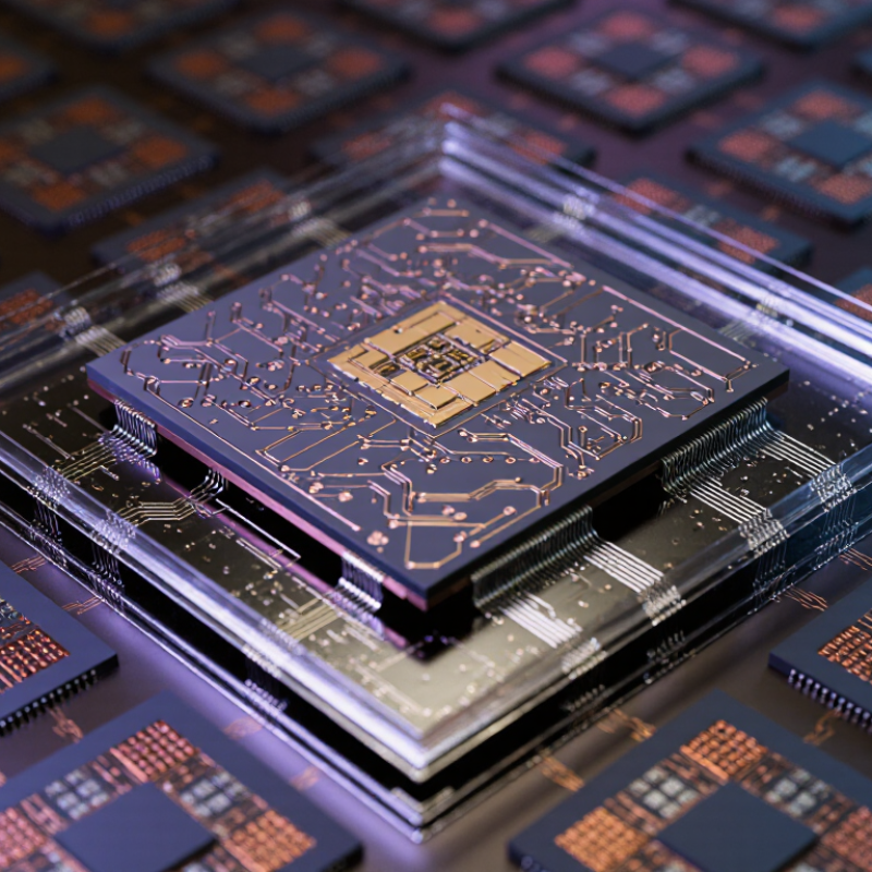
A monolithic integrated circuit is an electronic system built on one semiconductor die. Its definition rests on physical unity. Transistors, resistors, capacitors, and wiring form inside the same substrate during wafer fabrication. One die. Shared fabrication.
The silicon substrate provides the foundation, while microscopic doped regions control electrical behavior. Metal interconnect layers link these regions into amplifiers, memory cells, sensors, or processors. This arrangement shortens signal paths and reduces assembly points. It can improve speed, size, and reliability compared with circuits assembled from separate chips. However, “monolithic” does not mean every function works perfectly together. Heat, leakage, manufacturing variation, and limited material choices still shape performance.
Industry figures show why this architecture remains important. The World Semiconductor Trade Statistics Spring 2024 forecast valued the global semiconductor market at 611.2 billion dollars for 2024. An industry association reported 526.8 billion dollars in global semiconductor sales during 2023. These reports describe the wider market, not monolithic circuits alone. That distinction matters. Engineers should avoid treating broad market growth as proof that every monolithic design is optimal. In practical testing, a single-die circuit may reduce interconnect failures, yet one defective die can waste the entire component. Yield remains a difficult trade-off. Thermal behavior deserves equal attention. A compact package can simplify installation while concentrating heat in a small area.
| Concept or Dimension | Key Term | Accurate Description | Why It Matters |
|---|---|---|---|
| Basic Definition | Monolithic integrated circuit | A complete electronic circuit in which active devices, passive components, and their interconnections are fabricated together on a single semiconductor substrate. | Integrating many circuit elements on one substrate reduces physical size and eliminates numerous individual component connections. |
| Primary Substrate | Semiconductor wafer | The circuit is commonly formed in a thin semiconductor wafer, with silicon being the dominant material used for general-purpose integrated circuits. | The substrate provides the foundation for forming transistors, diodes, resistive regions, and isolation structures. |
| Active Components | Transistors and diodes | Transistors perform switching or amplification, while semiconductor diodes can provide rectification, protection, voltage references, or signal steering. | These devices provide the circuit's signal-processing and control functions. |
| Passive Components | Resistors and capacitors | Resistive and capacitive structures can be created within or above the semiconductor material using patterned doped regions, insulating layers, and conductive layers. | They support biasing, filtering, timing, feedback, energy storage, and signal conditioning. |
| Electrical Connections | On-chip interconnects | Metal or other conductive layers connect the fabricated devices according to the circuit layout, with insulating layers separating different wiring levels. | Integrated interconnects replace many external wires and enable compact, repeatable circuit construction. |
| Fabrication Principle | Planar processing | Modern monolithic circuits are generally produced through repeated sequences of deposition, photolithography, etching, oxidation or insulation, and controlled doping. | These processes allow microscopic device patterns to be reproduced across many circuit dies on a wafer. |
| Doping Function | Controlled impurity concentration | Selected regions of the semiconductor are modified with controlled impurity concentrations to create different electrical properties, including p-type and n-type regions. | Doping forms junctions and transistor structures required for current control and signal operation. |
| Circuit Scale | Integration density | The number of functional devices and interconnections on a die can range from a small number of elements to billions in highly complex digital circuits. | Higher integration density enables more functionality in a smaller area, although it increases design, manufacturing, and thermal-management complexity. |
| Typical Functions | Signal processing and control | Monolithic circuits may perform amplification, switching, logic operations, timing, voltage regulation, sensing, data conversion, or memory functions. | A wide range of functions can be implemented without assembling each transistor or passive component individually. |
| Main Advantages | Compactness and reliability | Important benefits include small size, low parasitic interconnection effects, low mass, consistent electrical characteristics, and high production repeatability. | These properties support reliable electronic systems with reduced assembly requirements and improved performance per unit area. |
| Main Limitations | Integration constraints | Some components, especially large inductors, high-value capacitors, high-power devices, and precision passive elements, may require substantial chip area or external components. | Not every circuit function is equally efficient to implement on one semiconductor die. |
| Thermal Consideration | Power density | As more devices operate within a small die area, the resulting heat generation and temperature distribution must be considered during circuit and package design. | Excessive temperature can affect performance, reliability, leakage current, and operating lifetime. |
| Testing Stage | Wafer and packaged-die testing | Electrical tests are performed on individual dies or packaged circuits to verify functionality, performance limits, and manufacturing quality. | Testing identifies defective or out-of-specification circuits before they are used in larger systems. |
| Packaging Relationship | Die versus package | The monolithic circuit is fabricated on the semiconductor die, while the package provides physical protection, external terminals, mechanical support, and often thermal paths. | The package is essential for practical use but is not the same as the monolithic circuit itself. |
| Core Distinction | Single-die integration | The defining feature is that the primary circuit elements are created together on one semiconductor die rather than being assembled as separate packaged components. | This single-die structure is the central idea behind the term “monolithic integrated circuit.” |